
The Nanoprobe beamline will focus hard X-rays at 60-300 nm length-scales, facilitating a broad range of X-ray investigations at the Australian Synchrotron. Multiple complementary contrast methods can be applied, often simultaneously, with the analytical volume defined by the volume of specimen illuminated by the focused beam. By scanning the specimen through the focus the Nanoprobe will map the properties of a specimen, including structure and composition, with resolution equal to the size of the focused spot.
Beamline Updates
Major contracts awarded & progress summary
| Work Package | Contractor | Status |
|---|---|---|
| Cryogenic Permanent Magnet Undulator (CPMU) | Proterial, SG Hitachi Metals, JP | Completed Installed |
| Front end (FE) | FMB-Berlin, DE | Completed Installed |
Hutches: First optical enclosure (FOE) Second optical enclosure (SOE) | Caratelli, FR - design and manufacture Lycopodium & Skilcon, AU - installation | Completed Services installed |
| Photon Delivery System (PDS) | Axilon, DE | FAT complete Installation underway |
| Nanoprobe Satellite Building (NSB) | CBD, AU - design arete, AU - build | Completed |
Endstation progress
| Endstation beam diagnostics | ANSTO in-house | Installation underway |
| Sample-KB table | Collab ANSTO & APS - concepts ANSTO - design, construct, commission | Delivered Installed |
| Kirkpatrick-Baez (KB) mirrors | SAES Getters (CINEL), IT | Delivered Installed |
| Delta robot | Collab ANSTO & DLS - concepts NH Micro - precision EDM flexures ANSTO - design, construct, commission | Commissioning |
| Detector gantry | ANSTO in-house | Installed |
SDD XRF detectors Xspress3X Mk II | RaySpec, UK Quantum Detectors, UK | Delivered SAT underway |
EIGER2 diffraction detectors On-axis detector vacuum vessel Off-axis detector industrial robot | Dectris, CH Fantini S.p.A, IT KUKA Robotics & CNCDesign, AU | Delivered, SAT completed Installation underway Installed, commissioning underway |
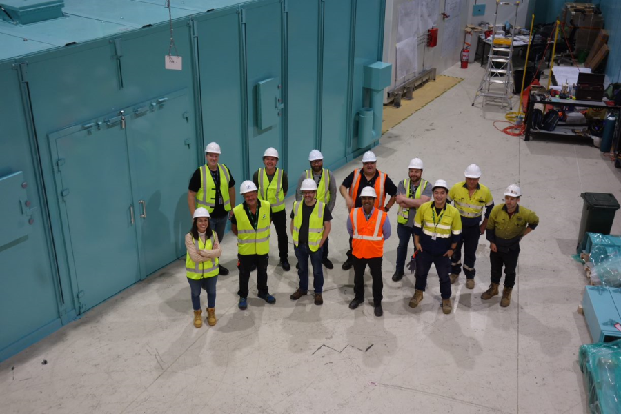
Hutches A & B
Nanoprobe and hutches teams pictured at the completion of Site Acceptance Testing (Mar 2023)
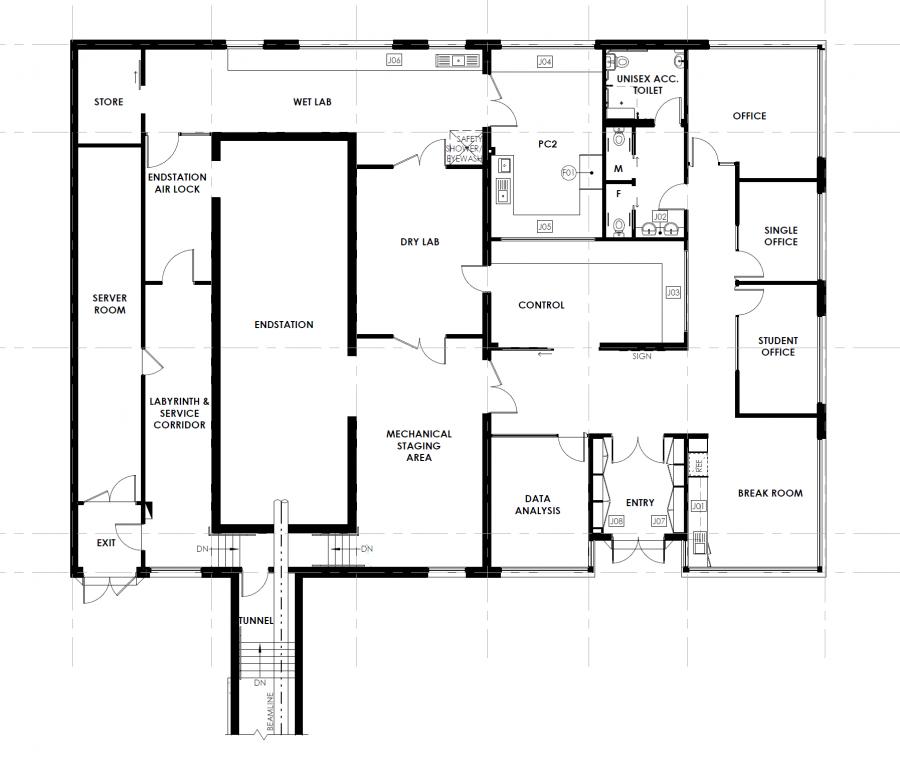
Nanoprobe Satellite Building (NSB) design
Design of the NSB was undertaken by CBD - Construction and Building Design Pty Ltd.
The floor plan is provided below. Special attention was paid to:
- multi-functional user laboratory spaces
- sample and User pathways
The building design takes into account mitigation strategies for:
- building drift relative to the Main Experimental Hall
- Endstation vibration susceptibility and isolation
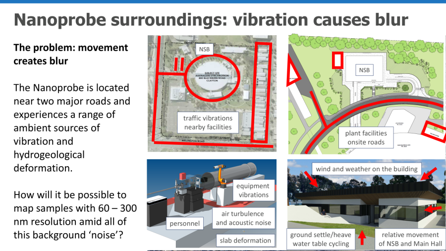
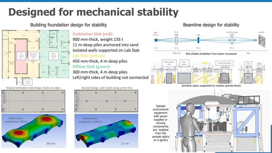
- Endstation thermal stabilisation
- Passive stabilisation

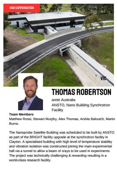
Nanoprobe Satellite Building (NSB) construction
Recently the NSB project was awarded a High Commendation at the 2025 Professional Excellence in Building Awards at the Chapter National Finalist Edition of the Australian Institute of Building Awards (July 2025)
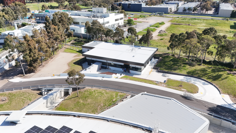
Aerial photograph (C. Millen - ANSTO) (Oct 2024)
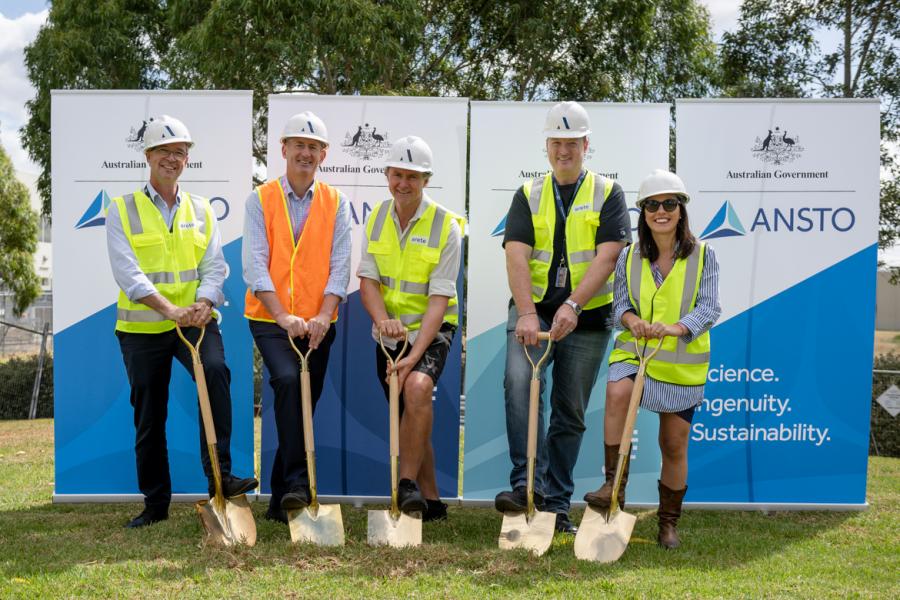
We are pleased to announce that arete Australia have been awarded the contract to construct the NSB (March 2023)
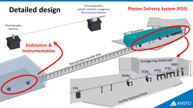
Photon Delivery System (PDS)
We are pleased to announce that Axilon have been awarded the contract to construct the Nanoprobe PDS!
PDR has been reached, with all major PDS components being agreed.
Below is a table indicating major components and their locations
| Component | Acronym | location along beamline [mm] |
|---|---|---|
| Fixed mask 1 | FM1 | 13,554 |
| White beam slits | WBS | 14,706 |
| Vertical focusing mirror | VFM | 15,852 |
| Horizontal focusing mirror | HFM | 16,552 |
| Beam imager 1 | BI1 | 17,433 |
| Fixed mask 2 | FM2 | 18,158 |
| Filters | FLT | 18,910 |
| Double multilayer monochromator | DMM | 19,868 |
| (Double crystal monochromator - deferred) | (DCM) | (20,953) |
| Beam imager 2 | BI2 | 21,946 |
| Fixed mask 3 | FM2 | 22,321 |
| Short transport line - FOE-SOE | ||
| Diamond quadrant beam position monitor | DBPM | 31,968 |
| Quad-diode beam position monitor | QBPM | 32,230 |
| Secondary source aperture | SSA | 32,630 |
| Beam imager 3 | BI3 | 33,190 |
| Monochromatic beam shutter | SHT | 33,765 |
| Fast vacuum valve | FVV | 34,319 |
| Long transport line - SOE-Endstation |
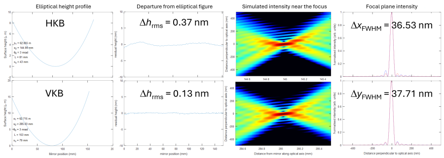
Nanofocusing Kirkpatrick-Baez Mirrors (Nano-KB)
Diffraction limited nanofocus simulated at 17.48 keV, incorporating metrology data from the actual mirrors fabricated by J-TEC:
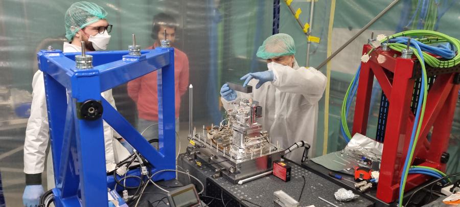
Nano-KB system at FAT @ CINEL (Apr 2024)
Nano-KB optics installation @ NANO Endstation (Nov 2025)
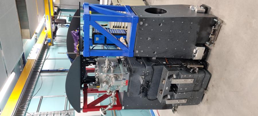
Endstation installation underway
Sample-KB table installed, KB mirrors installed, gantry installed, gantry axes undergoing commissioning.
Photo of NANO sample core (May 2025)
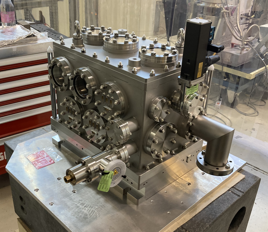
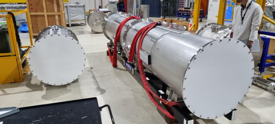
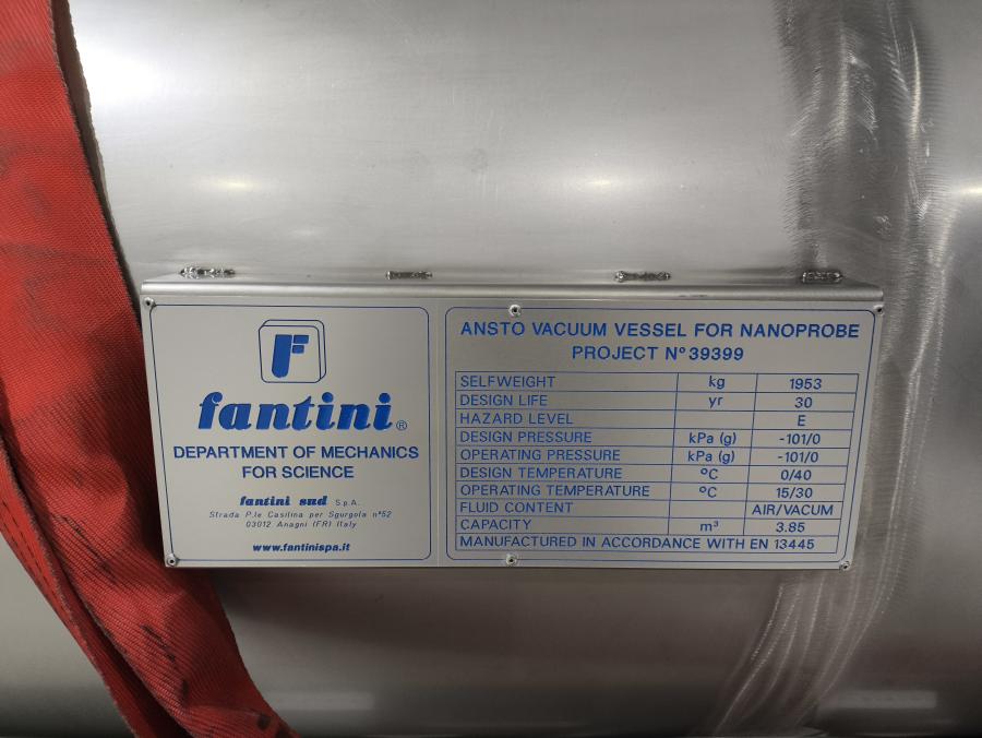
On-axis detector vessel
Delivered, moved to bull ring, undergoing vacuum leak testing.
Photos of the vessel after lifting into bull ring (Oct 2025)
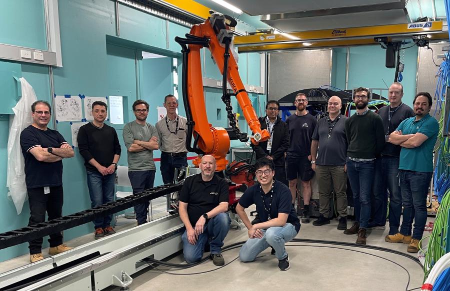
Off-axis robot
Delivered, installed, under commissioning.
Photograph of the off-axis robot installation team (Dec 2025)
Capability Summary and Techniques
Elemental mapping
Hard X-rays (5 keV – 20 keV) give the Nanoprobe unique analytical capabilities, revealing the elemental, chemical and structural information within specimens from a diverse range of scientific fields.
The size of the X-ray focus determines the spatial resolution of the Nanoprobe instrument; the intensity of the X-ray beam determines its sensitivity - the Nanoprobe targets 60-300 nm resolution and 1e10-1e13 ph/s intensity. The Nanoprobe beamline has been designed to enable resolution and sensitivity to be optimized for each investigation, enabling, e.g., improved elemental sensitivity at the cost of spatial resolution.
The Nanoprobe instrument will be optimized for elemental mapping using X-ray fluorescence in combination with scanning.
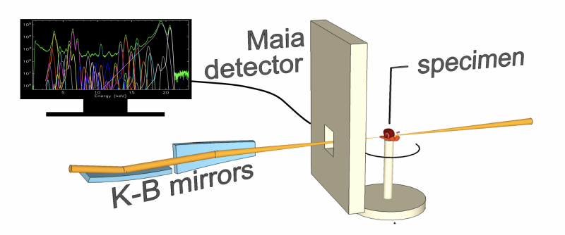
Elemental mapping using the Nanoprobe instrument.
An X-ray beam is focused onto a specimen using a KB mirror pair. In this figure, the focused beam passes through a Maia detector, positioned to capture the maximum amount of secondary photons emitted by the specimen.
The specimen is scanned through the beam, and at each position the Maia energy dispersive detector will be used to determine the energy of characteristic fluorescence X-rays emitted by the specimen, as well as Rayleigh and Compton scattered X-rays.
Super-resolution diffraction microscopy
In addition to elemental mapping, the Nanoprobe instrument will enable high-resolution visualization of a specimen’s phase and absorption using ptychography. An on-axis fast-framing hybrid pixel array records the X-ray intensity distribution downstream of the specimen as it is scanned through the beam. From this raw data, ptychography can build up structural images of the specimen at "super-resolution", i.e., smaller than the focused beam, anticipated down to around 15 nm. When high resolution is not required, or when the measurement conditions required for ptychography cannot be provided, differential phase contrast methods will be used to obtain at-resolution maps of phase and absorption.
Samples: type, preparation and presentation
- Scan range of 3 mm * 3 mm * 3 mm with sub-10-nm addressing precision.
- Typical specimen thickness will be below 10 µm. Thicker specimens may lose lateral imaging resolution due to projection overlay.
- A sample preparation laboratory is adjacent to the Endstation in the NSB, which is compatible with PC-2 certification (future upgrade) but this certification will not extend to the Endstation.
Off-line sample pre-alignment and characterization will be available.
The Nanoprobe beamline will enable key techniques including:
- Elemental mapping for most elements heavier than silicon (Si),
- Scanning Transmission and Differential Phase Contrast,
- Ptychography for phase and absorption contrast @ ~10-nm resolution,
- Tomography for all contrast modes
- DEFERRED upgrade: X-ray Absorption Near Edge Spectroscopy (XANES) will NOT be available until the DCM is installed. XANES provides chemical state analysis and mapping of elements ranging from Cr to Sr (K series), Ba to Bi (L series)
Future developments
In the first instance, radiation-induced specimen damage will not be mitigated. Pathways for upgrading the system to support cryogenics are encapsulated in the instrument design.
- A precision rotation stage will enable tomography with most measurement modes.
- Scanning nano-beam small- and wide angle X-ray scattering: nano-SAXS/WAXS
- Scanning nano-beam X-ray diffraction: nano-XRD
- An off-axis detector will enable Bragg-CDI and Bragg ptychography.
Scientific Applications
The Nanoprobe beamline will be able to address questions across a wide variety of scientific disciplines, including:
Human health and biology
First-row transition metals including manganese (Mn), iron (Fe), copper (Cu) and zinc (Zn) play key roles in biological systems, and are a co-factor in an estimated 30% of proteins. The Nanoprobe will provide a unique ability to map the distribution of these elements with high sensitivity and organelle-level resolution within biological systems such as cells and tissues to deliver insights into a range of questions in inorganic biochemistry with applications in eg mechanisms, pathology, and treatment of neurodegenerative diseases and other diseases of aging.
Food, agriculture, and plant biology
Micronutrients such as iron (Fe), copper (Cu), zinc (Zn) and selenium (Se) are essential to human nutrition. Simultaneously, toxic elements such as arsenic (As), cadmium (Cd) and lead (Pb) can be taken up by plants and so enter the food chain. Mapping the distributions of these elements within soils, fertilisers, root systems, stems and leaves will deliver insights into uptake, storage and biological fate of these metals and so enable improvements to the food chain with the potential to impact global food security.
Advanced materials and manufacturing
Nanomaterials technology is a key driver for manufacturing industry, and the Nanoprobe will provide a cutting-edge technique known as ptychography to provide high sensitivity imaging of larger nanoparticles at the 15 nm length scale. In addition, the ~60 nm X-ray probe will enable studies employing fluorescence, diffraction and scattering from small volumes within a specimen. The ability to employ both methods on a specimen within the one instrument will enable insights into nanostructure and function.
Environmental studies
Nanoscale distributions of environmental toxins are elucidated using the Nanoprobe. Examples include
- Distribution and speciation of toxic metals such as lead (Pb), mercury (Hg), and arsenic (As) in mine tailings and groundwater
- Uptake pathways afforded by plants
- Remediation pathways afforded by both plants and mineralogy
Earth Science and minerals formation
Mineralogy occurs across length-scales ranging from the nanometre to the kilometre. Providing insight bridging from the nanoscale to the microscale, the Nanoprobe will complement the XFM beamline (itself bridging the microscale to the decimetre scale) to provide a combination of detail and context that illuminates mineralogy and thus geological processes. Strategies for mining and exploration will be improved through studies of gold (Au), platinum (Pt), and uranium (U) bearing ore deposits, with the ability to probe chemical speciation providing key insights difficult if not impossible to obtain using other methods.
Cultural Heritage, Archaeology, and Arts
Understanding of the distribution and speciation of elements within art and artefacts can provide essential clues into origin, provenance, history, and genesis. Examples include:
- Chemical fingerprinting of ochres provides insights into the early Australian trading routes and so the extent of relations between aboriginal tribes.
- Chemical speciation studies of pigments in older paintings can greatly assist understanding of painting degradation and remediation
The applications of the Nanoprobe are very broad – this reflects the both the importance of metals to life and technology and the fact that you can put just about anything under a microscope! The unique capabilities of the Nanoprobe – exquisite elemental sensitivity, high resolution, high penetration – make it a key instrument for addressing nanoscale structure – function relations across a broad range of science. Taken from operating international facilities, specific examples of the kinds of measurements that we aim to deliver are listed below.
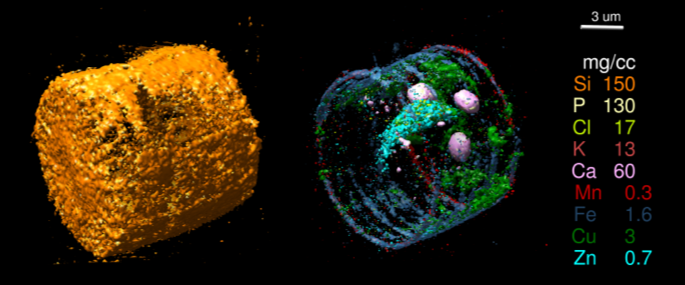
Elemental mapping at high resolution
Elemental distributions in frozen-hydrated Chlamydomonoas (green algae) measured using the Advanced Photon Source BioNanoprobe, alongside complementary ptychographic imaging.
From Deng et al, Scientific Reports (2017).
Ptychography for advanced nano-manufacturing and materials science: integrated circuits
Ptychography is a computationally-intensive method that provides access to high-resolution imaging, and will be able to resolve features down towards 15 nm with the Nanoprobe beamline.
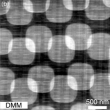
Ptychography of an integrated circuit fabricated with 16 nm technology. The apparent ‘hatching’ is due to these 16-nm vias and interconnects within the chip. Brighter colours indicate higher projected electron density.
Deng et al; Review of Scientific Instruments,90, 083701 (2019)
Elemental Mapping and Tomography
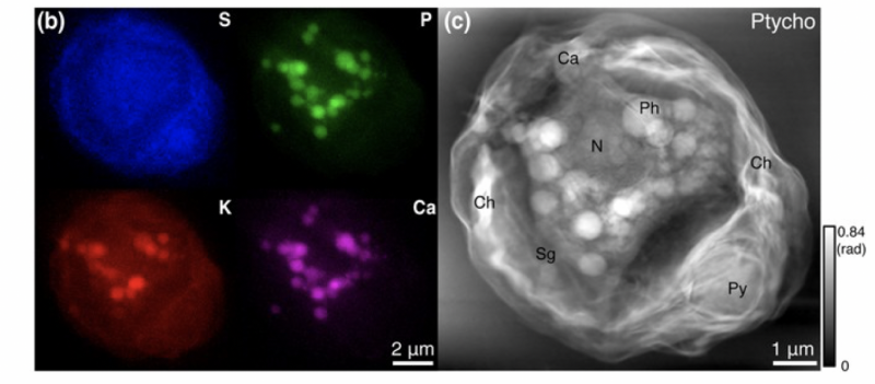
Elemental tomography of a diatom at 400-nm resolution reveals distribution of elements at micro-molar concentrations. We anticipate that such a measurement could be completed in one shift (8 hours) using the Nanoprobe. From de Jonge et al, PNAS (2010).
Mapping chemical co-ordination using XANES spectroscopy and imaging.
X-ray microprobes and nanoprobes are commonly used to perform local tests of chemical speciation (oxidation state), but the Nanoprobe will leverage world-leading expertise at the XFM beamline to deliver XANES imaging at the Nanoscale.
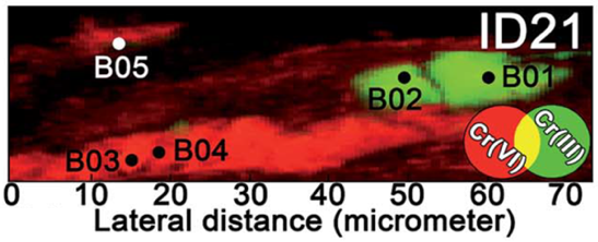
Imaging of chromium (Cr) speciation within a paint sample from van Gogh, showing alteration of Cr chemistry due to degradation. Data from the ESRF, ID21. From Monico et al, JAAS (2014).
Technical Information and Specifications
The Nanoprobe design allows the focused intensity to be traded against focal spot size for application to a wide variety of studies. At the highest resolution, roughly 108 ph/s will be focused into 60 nm; for measurements requiring higher intensity, roughly 1010 ph/s will be focused into 100 nm; highest sensitivity will focus roughly 1011 ph/s into 300 nm.
Several design features maintain the focused intensity on the Nanoprobe beamline, including:
- Use of a double multilayer monochromator (DMM) to transport the entirety of the undulator harmonic to the endstation at around 1% bandpass.
- Horizontal and vertical focusing to a Secondary Source Aperture (SSA) enables flux tuning with high dynamic range. This configuration also improves vibration resilience of the beamline transport.
- Kirkpatrick-Baez mirrors with high focusing efficiency and achromaticity will be used in the endstation.
Technical Specifications
View Nanoprobe Technical Specifications
| Function | Specific | Details |
|---|---|---|
| Insertion Device Source | CPMU |
|
| Monochromation | DMM |
|
| Nanofocusing optics | K-B mirrors |
|
| Scanning stages | Delta robot XYZ Smaract rotation Air-bearing granite Z |
|
| Fluorescence detectors | Silicon drift diodes (SDD) |
|
| On-axis detector | Hybrid pixel array EIGER2 XE 4M |
|
| Off-axis detector | Hybrid pixel array EIGER2 X 1M |
|
Beamline status & schedule
View Beamline status
| Date | Component / Stage |
| 2018 August | NANO - Preliminary design commences |
| 2020 April | NANO - Investment Case (IC) endorsed |
| 2020 June | NANO - Conceptual Design Report |
| 2020 July | NANO - NSB conceptual design commences |
| 2021 | NANO - Final Design Report |
| 2021 May | NSB design contract awarded (CBD) |
| 2022 January | Hutches contract awarded (Caratelli) |
| 2022 April | PDS contract awarded (Axilon) |
| 2022 June | CPMU contract awarded (Hitachi) |
| 2022 December | NSB construction contract awarded (arete) |
| 2023 January | KB mirror contract awarded to (Cinel) |
| 2023 March | PDS PDR (Axilon) |
| 2024 April | Nano KB Mirror system FAT @ CINEL |
| 2024 June | Nano KB Mirror optics received (JTEC) |
| 2024 July | NSB practical completion achieved (arete) |
| 2025 August | PDS FAT @ AXILON: Part 1 |
| 2025 December | PDS Delivery and Installation: Part 1 |
| 2026 May | PDS FAT Part 2 |
| (2026 June) | PDS Delivery and Installation: Part 2 |
| (2026 November) | Cold commissioning |
| (2027 February) | First Light to Endstation: Hot Commissioning commences |
| (2027 May) | "Day 1" Expert User operations and in-house commissioning |
| (2028 May) | "Day 365" Transition to full-time User operation |
Nanoprobe Schedule. Estimated overall COVID-19 delay: 9-months
Beamline layout
Find out more - Nanoprobe beamline User WIKI
Staff
- Mr Nader Afshar – Lead Controls Engineer
- Mr John Athanasakis – Senior Controls Engineer
- Mr Praneel Chugh – Controls Engineer
- Dr Evan Constable – Scientist
- Dr Martin de Jonge – Lead Scientist
- Mr Jim Divitcos – Design Engineer
- Dr Cameron M. Kewish – Senior Scientist
- Mr Craig Millen – Group Leader, Electrical Technicians
- Mr Callan Morey – Senior Mechanical Engineer
- Mr Saber Mostafavian – Lead Engineer (2024-)
- Dr Letizia Sammut – Senior Scientific Software Engineer
- Ms Michela Semeraro – Lead Engineer (2020-2024)
- Dr Prithi Tissa – Project Manager
- Mr Steve Truban – IT Systems Engineer
Mr Jason Wirthensohn – Senior Mechanical Technician
Beamline Advisory Panel
- Prof. Hugh Harris [Chair] – University of Adelaide
- Prof. Brian Abbey – La Trobe University
- Dr Louise Fisher – CSIRO
- Prof David Paganin – Monash University
- Dr Fatima Eftekhari [Retired] – Melbourne Centre for Nanofabrication
- Assoc Prof Mark Hackett – Curtin University
- Dr Alessandra Gianoncelli [International Advisor] – Sincrotrone Elettra, Italy
- Prof Stefan Vogt [International Design Advisor] – Argonne National Laboratory, USA